Innovative industrial collaborative research at WPI-NanoLSI

Takeshi Fukuma, Professor, Director, Nano Life Sciences Institute (WPI-NanoLSI), Kanazawa University
The Nano Life Science Institute (NanoLSI) at Kanazawa University was launched in October 2017 after the university was selected for the World Premier International Research Center Initiative of the Ministry of Education, Culture, Sports, Science and Technology. “A year or so has passed since the launch of NanoLSI and we are laying the ground work to achieve our goals of exploring mechanisms of biological phenomena at the nanoscale,” says Takeshi Fukuma, Director of the WPI-NanoLSI. “We have started to report some of our findings from this project as exemplified by the paper on self-sorting of pillar[n]arenes in Communications Chemistry based on the successful interdisciplinary collaboration between my colleagues Tomoki Ogoshi and Hitoshi Asakawa. Needless to say, academic research is a central part of this project. But we are also keen to expand collaboration with industrial partners. We have an excellent track record. I expect that such academia-industry interaction will increase as we start to publish and report more findings of research at WPI-NanoLSI.”
Fukuma has been working with industry for many years to solve specific problems such as ‘biofouling’ and metal corrosion using highly sophisticated AFM technology developed at Kanazawa. He has worked with an Australian company specializing in producing materials for coating buildings to prevent the adhesion of organic materials and so-called ‘biofouling’ by microorganisms. The company wanted to know why the materials they used were able to prevent certain bacteria and proteins from sticking to surfaces. So the company started to collaborate with researchers at a university in Australia but they could not understand the interface structure at the nano-level and requested to set up a joint project with Fukuma and colleagues to use the Kanazawa AFM technology. A student from the university spent a short time at Kanazawa to do some of the experiments. It was a really productive collaboration that led to deep insights into the ‘biofouling’ properties of materials as reported in their joint paper [Paul J. Molino et al, ACS Nano 2018]. “We have also been working with companies in Japan on metal corrosion that led to the development of the Open-Loop Electric Potential Microscopy system [Kyoko Honbo et al, ACS Nano 2016].”
Research highlights of industrial collaboration
Anti-fouling technology: 3D FM-AFM yields unprecedented insights into mechanisms governing fouling resistance of silicon nanoparticles to potentially harmful proteins, bacteria, and fungi.
Non-stick kitchen utensils are an example of technology that prevents adhesion of organic matter to surfaces. In the wider view, the development of effective technology for preventing the adhesion of bacteria and other so called ‘biofouling organisms’ to the surfaces of kitchenware, surgical instruments and other surfaces in medical care environments, and hulls of ships is an often invisible, but very important area of research with wide ranging social implications. For example, hospital related infections can lead to death, and slime and algae adhering to hulls of ships causes greater friction between the ship and water, leading to increases in fuel costs, and greater emission of pollutant gases into the atmosphere. These examples underscore that research on antifouling technology is important for benefit of society on a global scale.
Currently, toxic compounds containing heavy metals are widely used as antifouling coatings. But concerns about the impact of such compounds on the environmental and reports of the emergence of ‘biocide-resistant’ organisms have led to renewed efforts on research for new and innovative approaches for producing environmentally friendly anti-fouling materials. However, one of the major hurdles in this research is a lack of understanding of the basic mechanisms that govern the ability of certain materials, such as hydration layers, to prevent fouling, whilst other materials, for example with hydrophilic properties, do not show such behavior.
Here, Takeshi Fukuma and his group at Kanazawa NanoLSI collaborated with colleagues in Australia to study the main reasons for the anti-fouling behavior of silicon nanoparticles (SiNPs) functionalized with glycidoxypropyltrimethoxysilane (GPS-modified SiNPs) that have the potential of being candidates as next generation anti-fouling materials.
Specifically, the researchers used 3D frequency modulated atomic force microscopy (3D FM-AFM) to image the 3D structure of the interfacial water that covers SiNPs and measure forces experienced at nanometer distances above single SiNPs.
The FM-AFM technology developed at Kanazawa University by Fukuma and colleagues can detect single layers of water on surfaces such as mica, and notably, produce 3D spatial maps of the ion and energy distribution at a distance of only 2 nm above the surface. In this research, the AFM cantilever was positioned above single SiNPs located in a NaCl solution, to extract 3D images in the range 4 nm x 4 nm x 2 nm.
The main finding of this research was that interaction between chains of hydrophilic, epoxy organosilane groups on the surfaces of SiNPs with water molecules leads to the generation of a ‘quasi-stable’ layer that gives the SiNPs anti-fouling properties. These findings are expected to provide solid scientific basis for the development of other anti-foiling materials.
Reference
Hydration Layer Structure of Biofouling-Resistant Nanoparticles, Paul J. Molino†‡, Dan Yang†‡, Matthew Penna†§, Keisuke Miyazawa∥, Brianna R. Knowles†⊥, Shane MacLaughlin†⊥, Takeshi Fukuma∥∞ , Irene Yarovsky†§, and Michael J. Higgins†‡, ACS Nano 2018, 12, 11, 11610-11624.
Affiliations
† ARC Industrial Transformation Research Hub for Australian Steel Manufacturing, Wollongong, NSW 2522, Australia‡ ARC Centre for Electromaterials Science (ACES), Intelligent Polymer Research Institute/AIIM Faculty, Innovation Campus, Squires Way, University of Wollongong, Wollongong, NSW 2522, Australia
§ School of Engineering, RMIT University, Melbourne, Victoria 3001, Australia
∥ Division of Electronic Engineering and Computer Science and ∞Nano Life Science Institute (WPI-NanoLSI), Kanazawa University, Kakuma-machi, Kanazawa 920-1192, Japan
⊥ BlueScope Innovation Laboratories, Old Port Road, Port Kembla, NSW 2505, Australia
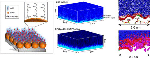
Illustration of the main findings reported in the paper.
Corrosion science: Open-loop electric potential microscopy offers a powerful means for directly imaging the distribution of corrosion cells on the surfaces of copper and stainless steel.
The corrosion of metals is major economic issue for industry. Obvious examples include stainless steel used to construct chemical and nuclear plants, another less known but equally important metal is copper that is used for forming electrical interconnections in the semiconductor manufacturing. Other metals include aluminum and light weight alloys widely used in the automobile and robotics sector.
Research to date based on electrochemical measurements has shown that corrosion of metals leads to the formation of ‘corrosion cells’ consisting of anodic and cathodic regions on the surfaces of metals. Electron microscopy and atomic force microscopy have yielded information about changes in the composition and structure of metals during corrosion. However, obtaining in-situ analysis and imaging of the formation of corrosion cells has been elusive.
Here, Takeshi Fukuma and members of his group at Kanazawa University collaborated with Ebara Corporation and Hitachi Ltd on the development of ‘open-loop electric potential microscopy’ (OL-EPM) for nanoscale imaging of corrosion cells. The measurements consist of applying a high frequency alternating current (AC) voltage between the tip of an AFM and the metal under investigation. The magnitude of the vibrations of the AFM tip are monitored and used to determine the electric potential at the surface.
This research focused on using OL-EPM for the direct imaging of the 2D distribution of local corrosion cells on the surfaces of copper wires and sensitized duplex stainless steel placed in electrolytic solutions of NaCl.
Two important findings of this research were that for copper, local corrosion cells initially formed between grains with different crystalline orientations and later were also observed at both the center and edges of the copper wires. In the case of the sensitized duplex steel, the OL-EPM imaging showed the existence of corrosion cells even in the absence of any changes to the structure of the surface.
OL-EPM offers a new approach for analysis of electrochemical reactions on the nanoscale for applications including metal corrosion as well as studying redox reactions in batteries and catalysis.
Reference
Visualizing Nanoscale Distribution of Corrosion Cells by Open-Loop Electric Potential Microscopy, Kyoko Honbo†‡, Shoichiro Ogata†, Takuya Kitagawa†, Takahiro Okamoto†, Naritaka Kobayashi†, Itto Sugimoto‡, Shohei Shima¶, Akira Fukunaga¶, Chikako Takatoh¶, and Takeshi Fukuma†§, ACS Nano 2016, 10, 2, 2575-2583.
Affiliations
† Division of Electrical Engineering and Computer Science, Kanazawa University, Kakuma-machi, 920-1192 Kanazawa, Japan
‡ Research and Development Group, Center for Technology Innovation – Materials, Hitachi, Ltd., 319-1292 Hitachi, Japan
¶ EBARA Corporation, 144-8510 Tokyo, Japan
§ ACT-C, Japan Science and Technology Agency, Honcho 4-1-9, 332-0012 Kawaguchi, Japan
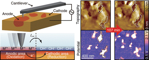
Schematic of corrosion reactions and OL-EPM.
Imaging charge accumulation: 3D open loop electric potential microscopy enables direct imaging of charge accumulation at interfaces of metals and electrolytes.
Nanoscale understanding of an electric double layer (EDL) that is formed at an electrode-electrolyte interface is important for developing electronic devices such as EDL capacitors and spintronic devices as well as for gaining insights into mechanisms governing corrosion and adhesion.
Here, Takeshi Fukuma and industrial partners at Ebara Corporation used the open-loop electric potential microscope (OL-EPM) developed at Kanazawa University for 3D imaging of accumulated charges in EDL for copper, platinum, and gold films in electrolytes.
Important results include successful visualization of opposite accumulation behaviors of Z-potential profiles with varying electric fields of polarizable and non-polarizable electrodes, and nanoscale distribution of charge accumulation at the interface of copper wire and electrolyte.
This research is expected to offer new methods for analyzing charge accumulation mechanisms for electronics and chemistry.
Reference
Visualizing charges accumulated in an electric double layer by three-dimensional open-loop electric potential microscopy, Kaito Hirata,a Takuya Kitagawa,a Keisuke Miyazawa,a Takahiro Okamoto,a Akira Fukunaga,b Chikako Takatohb and Takeshi Fukumaac, Nanoscale, 2018,10, 14736-14746.
Affiliations
aDivision of Electrical Engineering and Computer Science, Kanazawa University, Kakuma-machi, 920-1192 Kanazawa, Japan
bEBARA Corporation, 144-8510 Tokyo, Japan
cNano Life Science Institute (WPI-NanoLSI), Kanazawa University, Kakuma-machi, 920-1192 Kanazawa, Japan
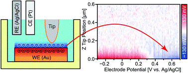
Measurement set up and an example of results